Introduction
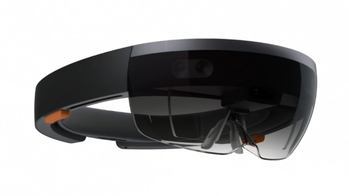
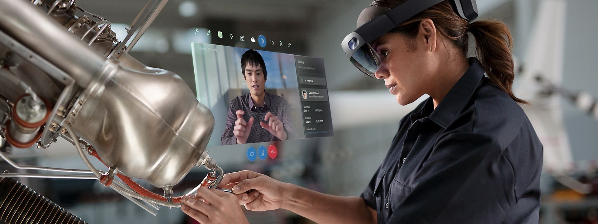
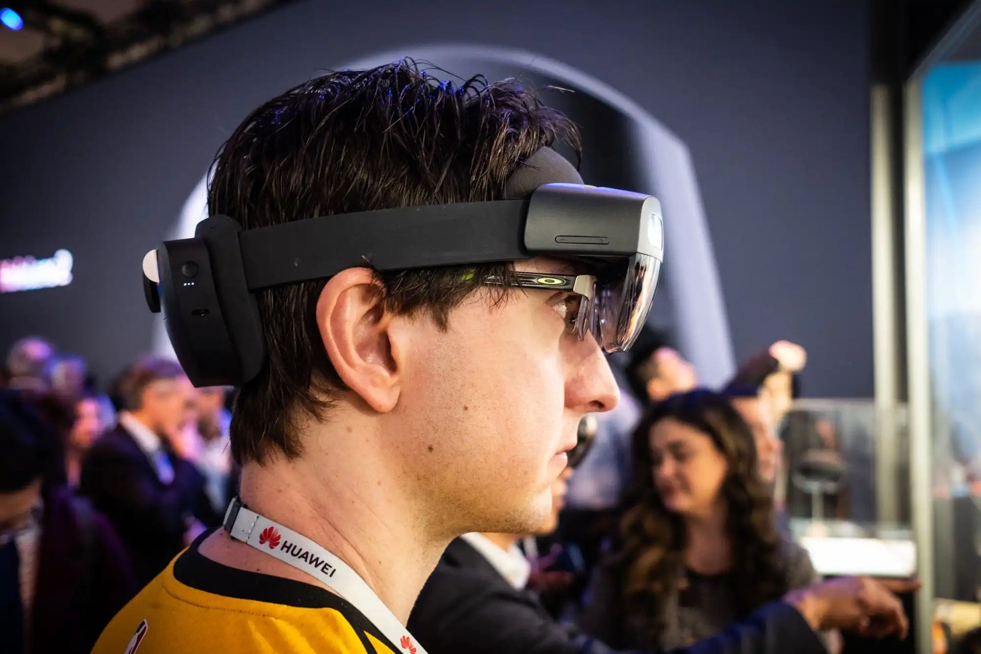
The HoloLens has revolutionized the way we experience augmented reality (AR) by seamlessly merging the digital and physical worlds. Developed by Microsoft, this cutting-edge device enables users to interact with holograms and digital content in a real-world environment. Behind the impressive capabilities of the HoloLens lies a complex system of components, with the chip being the heart and brain of the device.
This article will delve into the fascinating world of HoloLens chip technology, uncovering the key players involved in its development and the innovative processes used to create it. From the Microsoft Custom Holographic Processing Unit (HPU) to the collaboration with Qualcomm, Intel, and leading semiconductor manufacturers, we will explore how these partnerships have contributed to the advanced chip technology that powers the HoloLens.
By gaining insight into the ingenuity and collaboration behind the creation of the HoloLens chip, we can better appreciate the technical prowess that makes the device such a groundbreaking piece of technology. So, let’s dive into the intricacies of the HoloLens chip and discover the minds and machines responsible for its remarkable performance.
The HoloLens and Its Components
The HoloLens is a futuristic device that blends the physical and digital worlds through augmented reality. It consists of several crucial components that work together to deliver an immersive and interactive experience.
The first component of the HoloLens is the display system, which uses waveguides to project holographic images directly onto the user’s field of view. This allows users to see and interact with virtual objects seamlessly integrated into their surroundings. The display system is complemented by sensors that track the movements of the user’s head and eyes, ensuring that the holograms stay in the correct position regardless of their viewing angle or distance.
Another critical component of the HoloLens is the spatial sound system, which uses a combination of speakers and sensors to create a three-dimensional audio experience. This technology enables users to hear sound as if it is coming from specific directions in physical space, further enhancing the overall immersion.
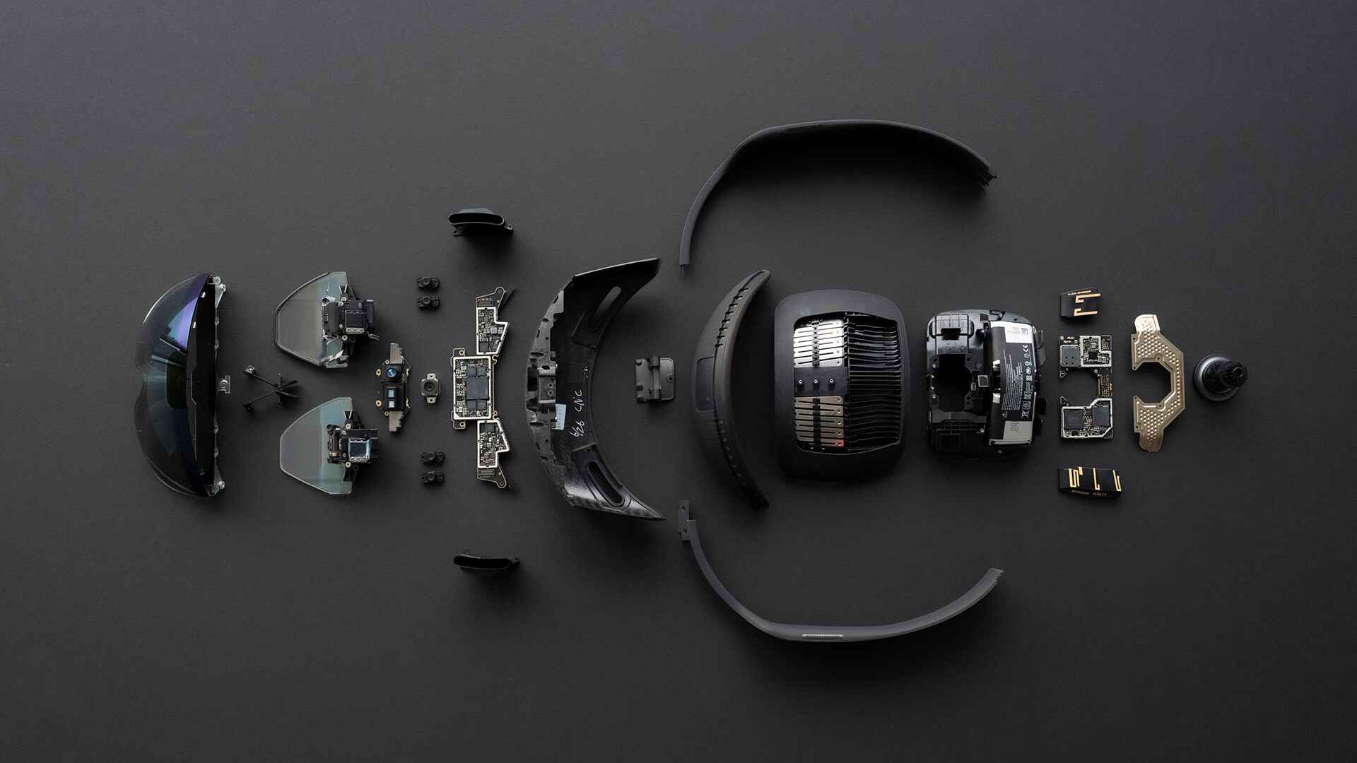
Powering all these components is the HoloLens chip, a technological marvel that enables fast and efficient processing of the device’s complex algorithms and graphics. The chip is responsible for rendering and projecting the holograms onto the waveguides, interpreting the input from sensors, and coordinating all the functionalities of the HoloLens.
Now that we have a basic understanding of the HoloLens and its components, let’s delve into the specifics of the chip technology that drives this exceptional AR device.
Overview of the HoloLens Chip
The HoloLens chip is a powerful piece of technology that fuels the entire augmented reality experience. It is responsible for processing and rendering the holographic content, tracking user movements, and coordinating various other functionalities of the device. To achieve this, the chip incorporates a combination of specialized processors and advanced manufacturing techniques.
At the heart of the HoloLens chip is the Microsoft Custom Holographic Processing Unit (HPU). This custom-designed chip combines both hardware and software components to deliver unparalleled performance and efficiency. The HPU is specifically optimized for holographic processing tasks, such as spatial mapping, gesture recognition, and voice command interpretation. Its dedicated circuitry enables real-time analysis of data from sensors, resulting in seamless interaction between the user and the holographic environment.
In addition to the HPU, the HoloLens chip also integrates a Qualcomm Snapdragon processor, known for its advanced mobile processing capabilities. The Snapdragon processor provides the computational power required to handle complex algorithms, graphics rendering, and wireless connectivity. This collaboration between Microsoft and Qualcomm ensures that the HoloLens can deliver smooth, responsive, and immersive augmented reality experiences.
To achieve the optimal performance and efficiency of the HoloLens chip, Microsoft has partnered with industry giants such as Intel, TSMC (Taiwan Semiconductor Manufacturing Company), and ASML (Advanced Semiconductor Materials Lithography). These collaborations aim to co-design and manufacture the chip using state-of-the-art manufacturing processes and techniques, maximizing its capabilities while minimizing power consumption and heat generation.
Through these partnerships and the integration of cutting-edge technologies, the HoloLens chip offers a powerful and efficient platform for augmented reality experiences. By continuously pushing the boundaries of chip design and manufacturing, Microsoft has created a device that sets new standards in the field of augmented reality.
Microsoft Custom Holographic Processing Unit (HPU)
The Microsoft Custom Holographic Processing Unit (HPU) is a key component of the HoloLens chip that plays a crucial role in delivering immersive augmented reality experiences. Developed by Microsoft, the HPU is a specialized chip designed specifically for holographic processing tasks, making it a core element of the HoloLens’ capabilities.
The HPU combines both hardware and software components to optimize holographic processing tasks, ensuring seamless interaction between the user and the holographic environment. It is responsible for various functions, including spatial mapping, gesture recognition, voice command interpretation, and real-time analysis of data from sensors.
The HPU’s dedicated circuitry enables efficient and real-time processing of sensory input from the HoloLens, allowing for precise and accurate tracking of user movements. This enables users to interact with holographic content seamlessly, as the HPU processes complex algorithms and interprets the user’s gestures and voice commands in real-time.
One of the significant advantages of the HPU is its ability to offload processing tasks from the main CPU, the Qualcomm Snapdragon processor in the case of HoloLens. This dedicated holographic processing capability ensures that the HoloLens operates smoothly and efficiently, without compromising on its other functionalities.
To develop the HPU, Microsoft combined its expertise in hardware design with deep learning, computer vision, and artificial intelligence algorithms. This fusion of disciplines allowed Microsoft to create a chip optimized for the specific demands of augmented reality experiences.
By designing a custom chip like the HPU, Microsoft has demonstrated its commitment to pushing the boundaries of technology and ensuring that the HoloLens delivers exceptional augmented reality experiences. The HPU’s dedicated holographic processing capabilities, combined with its integration with other components of the HoloLens chip, contribute to the device’s overall performance and cement its position as a leading augmented reality platform.
Qualcomm Snapdragon Processor
The Qualcomm Snapdragon processor is an integral part of the HoloLens chip, providing the computational power necessary to drive the device’s augmented reality capabilities. As a world-renowned leader in mobile processor technology, Qualcomm brings its expertise to the table to ensure optimal performance and efficiency in the HoloLens.
The Snapdragon processor is designed to handle the complex algorithms and graphics rendering required for augmented reality experiences. Equipped with multiple CPU cores, a powerful GPU, and advanced AI capabilities, the Snapdragon processor delivers the processing power necessary for seamless interaction with holographic content.
In addition to its processing prowess, the Snapdragon processor also plays a crucial role in enabling wireless connectivity on the HoloLens. With built-in Wi-Fi and Bluetooth technologies, the Snapdragon processor ensures that the HoloLens can connect to the internet, other devices, and cloud services, opening up a world of possibilities for collaborative and immersive experiences.
Qualcomm’s deep expertise in mobile processor design and optimization allows the Snapdragon processor to provide a balance between performance and power efficiency. This enables users to enjoy an extended and uninterrupted augmented reality experience without having to worry about battery drain.
Collaboration between Microsoft and Qualcomm ensures that the Snapdragon processor is integrated seamlessly into the overall architecture of the HoloLens chip. By working together, both companies optimize the coordination and communication between the HPU and the Snapdragon processor, enabling smooth and responsive augmented reality interactions.
The Snapdragon processor’s contribution to the HoloLens chip exemplifies the importance of partnerships between industry leaders. By combining Microsoft’s expertise in augmented reality and Qualcomm’s prowess in mobile processors, the HoloLens delivers an unparalleled user experience that sets the benchmark for augmented reality devices.
Collaboration with Intel
Microsoft’s collaboration with Intel has played a pivotal role in the development of the HoloLens chip, bringing together the expertise of both companies to create a powerful and efficient augmented reality platform. Intel’s contribution to the HoloLens chip technology lies in its expertise in semiconductor design, manufacturing processes, and optimization.
One significant area of collaboration between Microsoft and Intel is in the co-design of the chip architecture. By working closely together, the teams at both companies have been able to tailor the chip’s design to the specific requirements of the HoloLens, optimizing performance, power efficiency, and heat dissipation. This collaboration has resulted in a chip that can deliver the demanding processing tasks of augmented reality while maintaining an optimal user experience.
Intel’s manufacturing capabilities have also been instrumental in the HoloLens chip’s development. Intel utilizes advanced semiconductor manufacturing processes, such as its 10-nanometer process technology, to create chips with increased transistor density, reduced power consumption, and improved performance. This collaboration with Intel ensures that the HoloLens chip is not only powerful but also efficient, extending battery life and reducing heat generation.
Furthermore, Intel’s expertise in system integration has helped to optimize the performance and compatibility of the HoloLens chip with other components of the device. Intel’s focus on system-level integration allows for seamless communication and coordination between the various parts of the HoloLens, enhancing the overall user experience.
The collaboration between Microsoft and Intel extends beyond the technical aspects of chip development. Both companies have a shared vision of pushing the boundaries of technology and bringing innovative solutions to the market. This alignment of goals and values has created a strong partnership, driving continuous improvement and innovation in the field of augmented reality.
Through their collaboration, Microsoft and Intel have demonstrated the power of partnership in technological advancements. By leveraging each other’s strengths and expertise, they have successfully created a high-performance and efficient HoloLens chip that pushes the boundaries of augmented reality experiences.
Co-designing with TSMC and ASML
In addition to collaborating with Intel, Microsoft has also partnered with Taiwan Semiconductor Manufacturing Company (TSMC) and Advanced Semiconductor Materials Lithography (ASML) to co-design and manufacture the HoloLens chip. These collaborations bring together the expertise of these industry leaders in semiconductor manufacturing and lithography, ensuring the production of a high-performance and efficient chip.
TSMC, the world’s leading semiconductor foundry, plays a crucial role in the manufacturing of the HoloLens chip. Through their advanced manufacturing processes, TSMC produces chips with high transistor densities, allowing for increased processing power and efficiency. TSMC’s expertise in utilizing cutting-edge technology, such as the 7-nanometer fabrication process, contributes to the overall performance of the HoloLens chip.
ASML, on the other hand, provides critical lithography solutions that enable the production of highly precise and intricate chip designs. Lithography is the process of creating patterns on silicon wafers, and ASML’s advanced technology ensures the accuracy and reliability of these designs. Co-designing with ASML allows Microsoft to optimize the chip layout and ensure that the intricate features necessary for augmented reality processing are accurately replicated.
The collaboration between Microsoft, TSMC, and ASML goes beyond the manufacturing process. These partnerships involve close collaboration and coordination between the design teams at Microsoft and the engineers at TSMC and ASML. By working together from the initial design phase to the final manufacturing stage, these partners ensure that the HoloLens chip is optimized for performance, power efficiency, and manufacturability.
Co-designing with TSMC and ASML enables Microsoft to benefit from their deep knowledge and expertise in the semiconductor industry. These partnerships not only ensure that the HoloLens chip meets the highest quality standards but also help Microsoft stay at the forefront of technological advancements in the field of augmented reality.
Ultimately, the collaboration between Microsoft, TSMC, and ASML represents a synergy of efforts to develop and manufacture a state-of-the-art chip for the HoloLens. Through their combined expertise, these industry leaders have created a chip that delivers immense processing power, energy efficiency, and seamless integration with the rest of the HoloLens device.
Conclusion
The HoloLens chip stands as a remarkable feat of technological innovation, driving the immersive augmented reality experiences that define the HoloLens device. The collaboration with industry leaders such as Intel, Qualcomm, TSMC, and ASML has been instrumental in its development, showcasing the power of partnerships in pushing the boundaries of technology.
The Microsoft Custom Holographic Processing Unit (HPU) lies at the heart of the HoloLens chip, optimizing holographic processing tasks and enabling seamless interaction with holographic content. Its co-design with the Qualcomm Snapdragon processor ensures that the device delivers both powerful processing capabilities and wireless connectivity to the users.
Additionally, the collaboration with Intel has allowed for the co-design and optimization of the chip’s architecture, manufacturing processes, and system integration. The combination of Intel’s expertise in semiconductor design and manufacturing has resulted in a chip that operates with optimal performance, power efficiency, and heat dissipation.
TSMC and ASML’s contributions, through their advanced manufacturing processes and lithography solutions, have enabled the production of the HoloLens chip with high transistor densities and precise chip designs. Co-designing with these industry leaders has ensured that the chip meets the highest quality standards and remains at the cutting edge of technology.
The HoloLens chip, a result of these collaborations, has revolutionized the augmented reality landscape. Its powerful processing capabilities, seamless integration with other components, and energy efficiency combine to deliver immersive and interactive augmented reality experiences like never before.
As technology continues to advance, the HoloLens chip serves as a testament to the power of cooperation between companies with specialized expertise. Microsoft’s dedication to innovation and partnership has set the stage for a future of augmented reality that is both exciting and transformative.
In conclusion, the HoloLens chip is a remarkable achievement that showcases the pinnacle of technology and collaborative efforts. It has paved the way for the continued advancement of augmented reality, opening up a world of possibilities for immersive experiences in various fields, from gaming and entertainment to education and healthcare.